- 您现在的位置:买卖IC网 > Sheet目录3886 > PIC16F1827-I/ML (Microchip Technology)IC PIC MCU FLASH 4K 28-QFN
192
2570N–AVR–05/11
ATmega325/3250/645/6450
trol Unit will hold the SCL low until the slave is ready to receive more data. This may reduce the
actual data rate in two-wire mode.
21.3
Alternative USI Usage
When the USI unit is not used for serial communication, it can be set up to do alternative tasks
due to its flexible design.
21.3.1
Half-duplex Asynchronous Data Transfer
By utilizing the Shift Register in Three-wire mode, it is possible to implement a more compact
and higher performance UART than by software only.
21.3.2
4-bit Counter
The 4-bit counter can be used as a stand-alone counter with overflow interrupt. Note that if the
counter is clocked externally, both clock edges will generate an increment.
21.3.3
12-bit Timer/Counter
Combining the USI 4-bit counter and Timer/Counter0 allows them to be used as a 12-bit
counter.
21.3.4
Edge Triggered External Interrupt
By setting the counter to maximum value (F) it can function as an additional external interrupt.
The Overflow Flag and Interrupt Enable bit are then used for the external interrupt. This feature
is selected by the USICS1 bit.
21.3.5
Software Interrupt
The counter overflow interrupt can be used as a software interrupt triggered by a clock strobe.
21.4
Register Descriptions
21.4.1
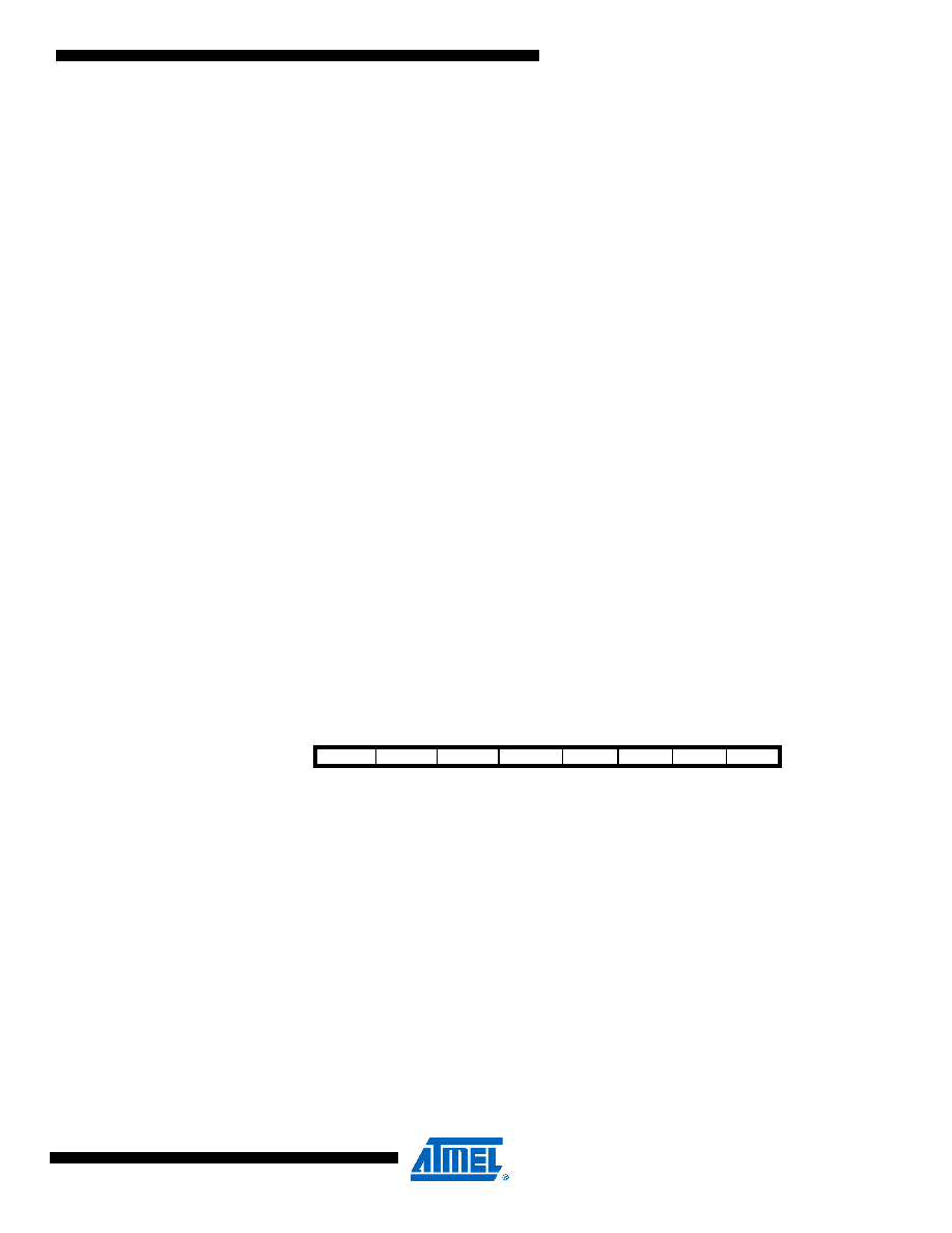
USIDR – USI Data Register
The USI uses no buffering of the Serial Register, i.e., when accessing the Data Register
(USIDR) the Serial Register is accessed directly. If a serial clock occurs at the same cycle the
register is written, the register will contain the value written and no shift is performed. A (left) shift
operation is performed depending of the USICS1..0 bits setting. The shift operation can be con-
trolled by an external clock edge, by a Timer/Counter0 Compare Match, or directly by software
using the USICLK strobe bit. Note that even when no wire mode is selected (USIWM1..0 = 0)
both the external data input (DI/SDA) and the external clock input (USCK/SCL) can still be used
by the Shift Register.
The output pin in use, DO or SDA depending on the wire mode, is connected via the output latch
to the most significant bit (bit 7) of the Data Register. The output latch is open (transparent) dur-
ing the first half of a serial clock cycle when an external clock source is selected (USICS1 = 1),
and constantly open when an internal clock source is used (USICS1 = 0). The output will be
changed immediately when a new MSB written as long as the latch is open. The latch ensures
that data input is sampled and data output is changed on opposite clock edges.
Bit
7
6
5
4
3
2
1
0
MSB
LSB
USIDR
Read/Write
R/W
Initial Value
0
发布紧急采购,3分钟左右您将得到回复。
相关PDF资料
PIC16LCE624T-04E/SO
IC MCU CMOS 1K OTP W/EEPRM18SOIC
PIC16LF1827-I/ML
IC PIC MCU FLASH 4K 28-QFN
PIC16LCE624-04E/SS
IC MCU CMOS 1K OTP W/EEPRM20SSOP
PIC16F687-I/P
IC PIC MCU FLASH 2KX14 20DIP
PIC16LF1829-I/SO
MCU PIC 14KB FLASH 20-SOIC
PIC16LCE624-04E/SO
IC MCU CMOS 1K OTP W/EEPRM18SOIC
PIC16F1829-I/SO
MCU PIC 14K FLASH 1K RAM 20SOIC
PIC16F685-I/SS
IC PIC MCU FLASH 4KX14 20SSOP
相关代理商/技术参数
PIC16F1827-I/MQ
功能描述:8位微控制器 -MCU 7KB Flash 384 byte 32 MHz Int. Osc RoHS:否 制造商:Silicon Labs 核心:8051 处理器系列:C8051F39x 数据总线宽度:8 bit 最大时钟频率:50 MHz 程序存储器大小:16 KB 数据 RAM 大小:1 KB 片上 ADC:Yes 工作电源电压:1.8 V to 3.6 V 工作温度范围:- 40 C to + 105 C 封装 / 箱体:QFN-20 安装风格:SMD/SMT
PIC16F1827-I/MV
功能描述:8位微控制器 -MCU 7KB Flash 384 RAM RoHS:否 制造商:Silicon Labs 核心:8051 处理器系列:C8051F39x 数据总线宽度:8 bit 最大时钟频率:50 MHz 程序存储器大小:16 KB 数据 RAM 大小:1 KB 片上 ADC:Yes 工作电源电压:1.8 V to 3.6 V 工作温度范围:- 40 C to + 105 C 封装 / 箱体:QFN-20 安装风格:SMD/SMT
PIC16F1827-I/P
功能描述:8位微控制器 -MCU 7KB Flash 384 byte 32 MHz Int. Osc RoHS:否 制造商:Silicon Labs 核心:8051 处理器系列:C8051F39x 数据总线宽度:8 bit 最大时钟频率:50 MHz 程序存储器大小:16 KB 数据 RAM 大小:1 KB 片上 ADC:Yes 工作电源电压:1.8 V to 3.6 V 工作温度范围:- 40 C to + 105 C 封装 / 箱体:QFN-20 安装风格:SMD/SMT
PIC16F1827-I/SO
功能描述:8位微控制器 -MCU 7KB Flash 384 byte 32 MHz Int. Osc RoHS:否 制造商:Silicon Labs 核心:8051 处理器系列:C8051F39x 数据总线宽度:8 bit 最大时钟频率:50 MHz 程序存储器大小:16 KB 数据 RAM 大小:1 KB 片上 ADC:Yes 工作电源电压:1.8 V to 3.6 V 工作温度范围:- 40 C to + 105 C 封装 / 箱体:QFN-20 安装风格:SMD/SMT
PIC16F1827-I/SS
功能描述:8位微控制器 -MCU 7KB Flash 384 byte 32 MHz Int. Osc RoHS:否 制造商:Silicon Labs 核心:8051 处理器系列:C8051F39x 数据总线宽度:8 bit 最大时钟频率:50 MHz 程序存储器大小:16 KB 数据 RAM 大小:1 KB 片上 ADC:Yes 工作电源电压:1.8 V to 3.6 V 工作温度范围:- 40 C to + 105 C 封装 / 箱体:QFN-20 安装风格:SMD/SMT
PIC16F1827T-I/ML
功能描述:8位微控制器 -MCU 7KB Flash 384 byte 32 MHz Int. Osc RoHS:否 制造商:Silicon Labs 核心:8051 处理器系列:C8051F39x 数据总线宽度:8 bit 最大时钟频率:50 MHz 程序存储器大小:16 KB 数据 RAM 大小:1 KB 片上 ADC:Yes 工作电源电压:1.8 V to 3.6 V 工作温度范围:- 40 C to + 105 C 封装 / 箱体:QFN-20 安装风格:SMD/SMT
PIC16F1827T-I/MQ
功能描述:8位微控制器 -MCU 7KB Flash 384 byte 32 MHz Int. Osc RoHS:否 制造商:Silicon Labs 核心:8051 处理器系列:C8051F39x 数据总线宽度:8 bit 最大时钟频率:50 MHz 程序存储器大小:16 KB 数据 RAM 大小:1 KB 片上 ADC:Yes 工作电源电压:1.8 V to 3.6 V 工作温度范围:- 40 C to + 105 C 封装 / 箱体:QFN-20 安装风格:SMD/SMT
PIC16F1827T-I/MV
功能描述:8位微控制器 -MCU 7KB Flash 384 RAM RoHS:否 制造商:Silicon Labs 核心:8051 处理器系列:C8051F39x 数据总线宽度:8 bit 最大时钟频率:50 MHz 程序存储器大小:16 KB 数据 RAM 大小:1 KB 片上 ADC:Yes 工作电源电压:1.8 V to 3.6 V 工作温度范围:- 40 C to + 105 C 封装 / 箱体:QFN-20 安装风格:SMD/SMT